

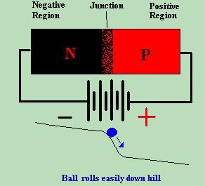
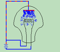
 Recall that in a semiconductor diode, we have 2 regions of DOPED semiconductive material. One region is doped positive, and the other region is doped negative. There is also a junction, where the two regions are joined. Recall that in a semiconductor diode, we have 2 regions of DOPED semiconductive material. One region is doped positive, and the other region is doped negative. There is also a junction, where the two regions are joined.When a diode is forward biased, it conducts electricity easily, like a ball rolling down a hill. When it is reverse biased, it is extremely resistive to current flow, as the ball is rolling uphill, and is much harder to get over the hump. Remember also, that we had diode tubes, which operated in a similar manner. They would conduct electricity in one direction easily, but would not conduct in the opposite direction. When we added another element to a tube, we created a triode, which would not only allow electricity to flow, but could also amplify the signal. Reason tells us that if we add another element to a semiconductor diode, that a similar effect should take place. In December of 1947, Scientists at Bell Laboratories would prove this theory correct. 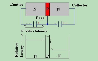 With the addition of a 3rd semiconductive layer, joined at a second P-N junction, W. H. Brattain made the world famous comment, " We've Got Gain! " implying that this 3 layer device could amplify! With the addition of a 3rd semiconductive layer, joined at a second P-N junction, W. H. Brattain made the world famous comment, " We've Got Gain! " implying that this 3 layer device could amplify! With proper bias applied, there is a small hill to overcome at the first P-N junction (approximately 0.7 Volts for Silicon, 0.3 Volts Germanium), which is the normal characteristic for any semiconductor diode. But then the electrons reach the peak of the hill at the second P-N junction, and have a fast run downward. There is an increase in flow downhill, and the electrons act like a waterfall, pouring into the collector. It may seem at first, that a transistor is like 2 diodes placed back to back, and in resistance checks will even resemble this. Actually though, 2 diodes back to back will not operate like a transistor in circuit. Of the many kinds of transistors there are, probably the most commonly used is the Small Signal, Bipolar transistor, as pictured above. Bipolar transistors come in two flavors: PNP and NPN. This is because the semiconductive material can be laid out in ( basically ) two different ways. 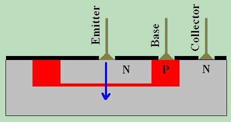 If we look closely at how a bipolar transistor is made, we can understand more easily how this can be. The illustration to the left is a cutaway of a semiconductor transistor. Try to visualize this as being circular ( button shaped ) from the top view, with 3 layers, one upon another. If we look closely at how a bipolar transistor is made, we can understand more easily how this can be. The illustration to the left is a cutaway of a semiconductor transistor. Try to visualize this as being circular ( button shaped ) from the top view, with 3 layers, one upon another.Transistors are built in layers by very precise machines. Each layer is added to the layer below it. We begin with a single layer ( or substrate ), and add layers on top of it. If we begin with a layer of N type semiconductor ( on the bottom ), the second layer would be P type, followed by another N type. We say that transistors, and other semiconductive devices, are "grown" in this manner. The second layer ( in this case a P type ), is very thin, along the order of 800 micrometers ( μM ) or less. As shown by the blue line, electric current enters via the N type emitter substrate layer, passes through the ( red ) P type base substrate layer, until it reaches the N type collector substrate layer. The gold colored lines represent the leads that connect the transistor to outside circuitry. If we were to reverse the N and P layers, we would have a PNP transistor, with the base being N type, and the emitter and collector being P type material. 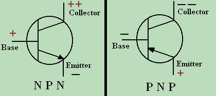 The schematic diagram symbol for a bipolar transistor is shown to the right. Notice that the only difference between an NPN and PNP type transistor, is the direction of the arrow. To remember which is which, just keep in mind that the NPN is Not Pointing to the base. The schematic diagram symbol for a bipolar transistor is shown to the right. Notice that the only difference between an NPN and PNP type transistor, is the direction of the arrow. To remember which is which, just keep in mind that the NPN is Not Pointing to the base. ( NP = Not Pointing ) Otherwise, the two symbols are identical. The EMITTER is ALWAYS the ARROW, the base is always the line ( think baseline ), and the collector is the one left over. What we haven't covered yet, is other semiconductor devices, like the Silicon Controlled Rectifier, Field Effect Transistor, as well as multicircuit microchips, logic circuits, and microprocessors. |
| (On The Following Indicator... PURPLE will indicate your current location) | ||||||||||||||||||||||||
| 1 | 2 | 3 | 4 | 5 | 6 | 7 | 8 | 9 | 10 | 11 | 12 | 13 | 14 | 15 | 16 | 17 | 18 | 19 | 20 | 21 | 22 | 23 | 24 | 25 |
| 26 | 27 | 28 | 29 | 30 | 31 | 32 | 33 | 34 | 35 | 36 | 37 | 38 | 39 | 40 | 41 | 42 | 43 | 44 | 45 | 46 | 47 | 48 | 49 | 50 |
| 51 | 52 | 53 | 54 | 55 | 56 | 57 | 58 | 59 | 60 | 61 | 62 | 63 | 64 | 65 | 66 | 67 | 68 | 69 | 70 | 71 | 72 | 73 | 74 | 75 |
[COURSE INDEX] [ELECTRONICS GLOSSARY] [HOME]
| Otherwise - please click to visit an advertiser so they know you saw their ad! |
