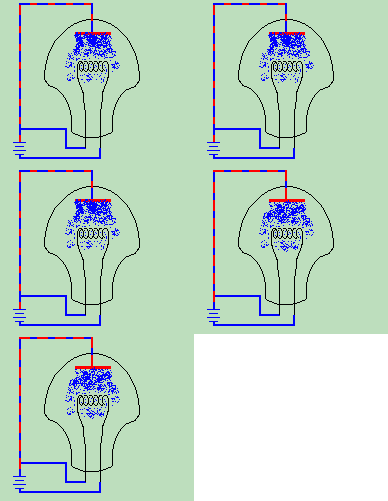
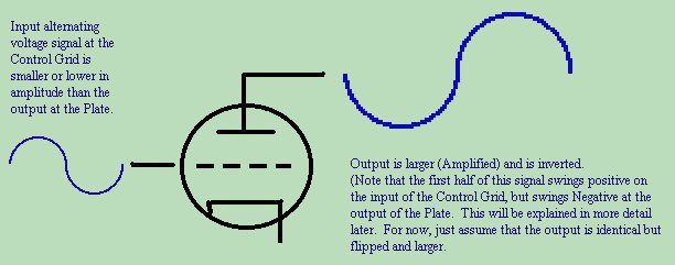
 You may or may not recall that when a signal goes into an amplifier, it tends to come out inverted. Let us now apply that to a logic circuit. Instead of having a nice pretty sine wave - we have ones and zeros. (5V and 0V / Saturated and Cut-Off). If we INVERT that - then with a high coming into the transistor, we have a low going out of the transistor. Alternately - with a low going into the transistor, we have a high coming out of the transistor. If we were to plot that on a logic chart - we would quickly discover that an amplifier (whether it be a tube, bipolar transistor, or Field Effect Transistor), by the very nature of how it works - is a NOT GATE!
Now you know the crux of the problem with digital logic. You can't just use diodes and resistors, as the signal degrades. You need amplification. But when you amplify, the amplifying device acts as a NOT gate. How then do you make a standard AND gate with transistors or tubes? Well, it is a bit of a cludge - but what you have to do is build a NAND gate followed by a NOT gate. What in the blue moon is a NAND gate? Well, it is a gate that acts like an AND gate followed by a NOT gate, so the output will wind up being exactly the opposite of what you want. So you simply follow it with another NOT gate to fix the problem. Perhaps pictures will help.

A NOT gate in electronics is also called an INVERTER. It is called that because whatever you put into it, it inverts (turns upside down) the signal, giving an output that is opposite from the input. A NAND gate is an AND gate with a NOT gate immediately following it. Because of this - whatever the output of an AND gate woudl be - the NAND gate would have the OPPOSITE output.
| A |
AND |
B |
YIELDS |
OUTPUT |
| 0 |
∧ |
0 |
→ |
0 |
| 0 |
∧ |
1 |
→ |
0 |
| 1 |
∧ |
0 |
→ |
0 |
| 1 |
∧ |
1 |
→ |
1 |
|
|
| A |
NAND |
B |
YIELDS |
OUTPUT |
| 0 |
¬∧ |
0 |
→ |
1 |
| 0 |
¬∧ |
1 |
→ |
1 |
| 1 |
¬∧ |
0 |
→ |
1 |
| 1 |
¬∧ |
1 |
→ |
0 |
|
After you let all that soak in - let's figure out how to build a NAND gate!
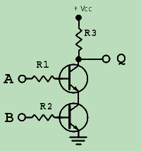 Input comes in on A and B. Depending on the input, the output goes out on Q as per the table above. This shouldn't be a hard concept for you by now. Assuming that you have a High on B, it turns on the bottom transistor, putting a low on its output - in essence - a ground. Then assuming you also have a high on A, it also turns on, allowing a ground on the output of the top transistor. So in order to have a low (zero Volts) on the output of the top transistor - you need to have a high on both pins A and B, otherwise, there is an open circuit, and whatever voltage exists at the top of R1, is also seen at the bottom of R1 (which is the output of the top transistor). Problem is that if you want an AND gate instead of a NAND gate, you have to follow it with a NOT gate.
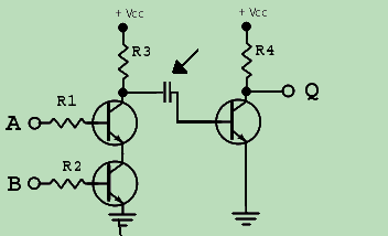 So we build a circuit something like this one. Note that we show a capacitor between the "two" circuits (the NAND and the NOT). This is shown for coupling purposes. By the same token, it could possibly be resistively coupled, or perhaps even directly coupled. The key point here is that you can't build an AND gate with just 2 transistors - you need the third to "invert" the signal.
If we can create an AND gate from a NAND gate - then creating an OR gate shouldn't be a problem - if we can make a NOR gate. And of course - we can.
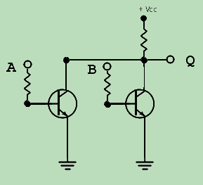 As you can see from the diagram on the right, data signals come in on inputs A and B respectively. A high on A causes the transistor to conduct. With the emitter at ground, and the collector resistor at a very high level of resistance, the output of the transistor gets sucked down to a low. Same applies for B. So with 2 highs going in, you have a low coming out. On the other hand, given a low on A, the transistor does not conduct at all, and acts as an open. With an open on the transistor, the VCC is seen at the bottom side of the collector resistor, and thus at Q. Putting a not gate at the output of Q turns it into an OR gate.
So far we've studied relay logic, and what is called RTL logic (Resistor-Transistor Logic). There is also TTL logic (Transistor-Transistor Logic), and various other kinds of logic gates. RTL has its good and bad points. Drawbacks of RTL logic is that it has resistors, which use energy and generate noise, thus making for slower, less reliable, higher heat generating, and more energy using circuitry. Good point is that it is easy to build from scratch, and a great educational tool!
The main point though - whether we are using tubes, transistors, MOSFETS or whatever amplifying device (or even relays), is that you understand the basics of how logic circuits work. From there you can play with, and learn other types of logic circuits. We started with AND, NOT, and OR logic statements. Now you are familiar with NAND and NOR gates as well. Of course gates like the AND and OR are not simply limited to 2 inputs. You can have a 256 input or gate if you want to. There are also gates like "Exclusive Or" gates, etc. which I may cover in another course specifically on digital logic.
The gates you have learned are joined in series (cascaded) or parallel in order to create more sophisticated circuitry, which make up the brains of the computer you use. Using ones and zeros, the computer can make simple decisions at a rate of millions per second.
|


