

|
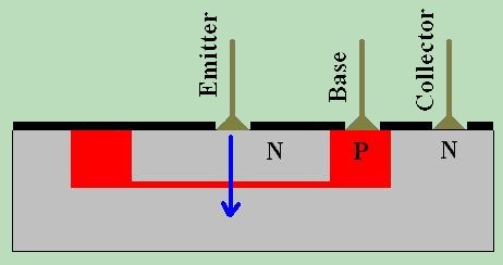
Way back in 1945, Shockley had an idea for making a solid state amplifying device out of semiconductors. He reasoned that if you had a strong electrical FIELD, you could cause the flow of electricity within a nearby semiconductor. He tried to build one himself, but failed. He also had Walter Brattain attempt to make one - but again it didn't work. Along the way, they came across a partial success - the bipolar junction transistor we've already studied. But it didn't work quite the way they expected. The thought was that the semiconductor device should work identical in nature to a vacuum tube. It didn't. But when the words "This thing's got Gain!" were first uttered, the world would never be the same. It wouldn't happen until nearly 20 years later, still in Bell Labs, that John Atalla would be trying to make Shockley's ideas come to life, when a new semiconductor device would come about - the Field Effect Transistor. This device worked much more like tubes, and in many cases, were lower voltage replacements in similar circuitry!  Taking the bipolar transistor for a ride, we'll discuss now how the Field Effect Transistor is made, and how it works. If you look at the bipolar transistor to the right, you notice that it is built in Layers. These layers are called "substrates". Taking the bipolar transistor for a ride, we'll discuss now how the Field Effect Transistor is made, and how it works. If you look at the bipolar transistor to the right, you notice that it is built in Layers. These layers are called "substrates".
A very large crystalline structure is formed in a very high temperature oven. It is then sliced into disks or wafers. Each wafer is then spun coated with a photo sensitive layer, then is "developed" using the semiconductor equivalent to a photographic developer (basically an overgrown overhead projector on steroids). The light sensitive layer is then washed away with a chemical bath - also similar to how a photograph is made. It is then doped, and copper is added as needed. Finally, it is shaved down, cut into sections and you get what you see to the right. A layered "chip" of silicone with just the right impurities to make it do its job.
In the FET, we find a doped piece of semiconductor material with 3 electrodes attached to the TOP: One to the middle Positive section - called the Gate. One to each of the two Negative sections, called the Source and Drain respectively. Under the Positive doped section is another negative doped section called the "substrate". By applying a voltage to the source and drain electrodes, current will flow through it. The side where the electrons come in is known as the source, and corelates to the anode of a tube. The side where the electrons go out is called the drain, and coresponds to the Plate of a tube. Cut Off and Saturation are not normally considered a good thing. To an analog signal, like your favorite music, it will cause distortion, as the tops and/or bottoms of the sine waves are removed. This gives a very bad sound. There are conditions, however, when cutoff or saturation are considered a good thing. If we are simply building a switching circuit that needs to turn on and off, then "signal quality" is not necessarily as important as "state". In that case, it may conserve energy to run the FET "switch" in saturation and cutoff all the time. The two most common forms of FET are the JFET (Junction FET) and the MOSFET (Metal Oxide Semiconductor FET). They both work in the "depletion zone" method as described above, but each has its own flavor of pros and cons. |

| (On The Following Indicator... PURPLE will indicate your current location) | ||||||||||||||||||||||||
| 1 | 2 | 3 | 4 | 5 | 6 | 7 | 8 | 9 | 10 | 11 | 12 | 13 | 14 | 15 | 16 | 17 | 18 | 19 | 20 | 21 | 22 | 23 | 24 | 25 |
| 26 | 27 | 28 | 29 | 30 | 31 | 32 | 33 | 34 | 35 | 36 | 37 | 38 | 39 | 40 | 41 | 42 | 43 | 44 | 45 | 46 | 47 | 48 | 49 | 50 |
| 51 | 52 | 53 | 54 | 55 | 56 | 57 | 58 | 59 | 60 | 61 | 62 | 63 | 64 | 65 | 66 | 67 | 68 | 69 | 70 | 71 | 72 | 73 | 74 | 75 |
[COURSE INDEX] [ELECTRONICS GLOSSARY] [HOME]
| Otherwise - please click to visit an advertiser so they know you saw their ad! |
